.site-title, .site-description { position: absolute; clip: rect(1px, 1px, 1px, 1px); }

Comprehensive comparison and engineering application analysis of alumina, zirconia, silicon carbide and silicon nitride ceramics coated alumina

Material Overview

Advanced structural ceramics, due to their special crystal structure and chemical bond qualities, show efficiency advantages that metals and polymer materials can not match in severe settings. Alumina (Al Two O FIVE), zirconium oxide (ZrO ₂), silicon carbide (SiC) and silicon nitride (Si ₃ N FOUR) are the 4 major mainstream engineering porcelains, and there are essential differences in their microstructures: Al ₂ O five comes from the hexagonal crystal system and depends on strong ionic bonds; ZrO two has 3 crystal forms: monoclinic (m), tetragonal (t) and cubic (c), and obtains unique mechanical residential properties via phase change toughening mechanism; SiC and Si Five N ₄ are non-oxide ceramics with covalent bonds as the primary element, and have more powerful chemical stability. These architectural distinctions straight result in considerable differences in the preparation process, physical buildings and design applications of the four. This article will systematically examine the preparation-structure-performance relationship of these 4 porcelains from the viewpoint of products science, and discover their potential customers for commercial application.
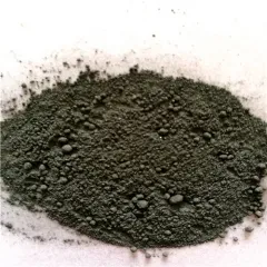

(Alumina Ceramic)

Prep work procedure and microstructure control

In terms of preparation procedure, the four ceramics show apparent distinctions in technological routes. Alumina porcelains make use of a fairly traditional sintering procedure, generally using α-Al two O five powder with a purity of greater than 99.5%, and sintering at 1600-1800 ° C after dry pressing. The secret to its microstructure control is to prevent unusual grain development, and 0.1-0.5 wt% MgO is typically added as a grain limit diffusion prevention. Zirconia ceramics need to present stabilizers such as 3mol% Y TWO O five to maintain the metastable tetragonal stage (t-ZrO ₂), and utilize low-temperature sintering at 1450-1550 ° C to prevent excessive grain growth. The core procedure obstacle hinges on precisely controlling the t → m phase transition temperature level window (Ms factor). Given that silicon carbide has a covalent bond proportion of up to 88%, solid-state sintering requires a high temperature of greater than 2100 ° C and relies upon sintering help such as B-C-Al to create a fluid phase. The response sintering method (RBSC) can accomplish densification at 1400 ° C by penetrating Si+C preforms with silicon melt, but 5-15% complimentary Si will certainly continue to be. The preparation of silicon nitride is the most complicated, generally using GPS (gas pressure sintering) or HIP (hot isostatic pushing) processes, including Y TWO O SIX-Al two O six collection sintering aids to form an intercrystalline glass stage, and warmth treatment after sintering to crystallize the glass stage can considerably boost high-temperature performance.


( Zirconia Ceramic)

Contrast of mechanical buildings and strengthening device

Mechanical properties are the core evaluation indicators of architectural ceramics. The 4 sorts of products show entirely different conditioning systems:


( Mechanical properties comparison of advanced ceramics)

Alumina mainly relies upon great grain strengthening. When the grain size is decreased from 10μm to 1μm, the stamina can be enhanced by 2-3 times. The superb strength of zirconia comes from the stress-induced stage improvement system. The stress and anxiety field at the split tip sets off the t → m stage makeover accompanied by a 4% volume expansion, leading to a compressive stress and anxiety securing impact. Silicon carbide can enhance the grain boundary bonding stamina with solid service of elements such as Al-N-B, while the rod-shaped β-Si four N four grains of silicon nitride can create a pull-out impact similar to fiber toughening. Crack deflection and connecting contribute to the renovation of toughness. It is worth keeping in mind that by creating multiphase ceramics such as ZrO TWO-Si Six N ₄ or SiC-Al Two O SIX, a range of strengthening mechanisms can be coordinated to make KIC exceed 15MPa · m ¹/ TWO.

Thermophysical homes and high-temperature actions

High-temperature security is the key benefit of structural ceramics that differentiates them from traditional materials:


(Thermophysical properties of engineering ceramics)

Silicon carbide displays the most effective thermal management performance, with a thermal conductivity of up to 170W/m · K(equivalent to aluminum alloy), which results from its easy Si-C tetrahedral structure and high phonon breeding rate. The low thermal expansion coefficient of silicon nitride (3.2 × 10 ⁻⁶/ K) makes it have excellent thermal shock resistance, and the crucial ΔT worth can reach 800 ° C, which is specifically appropriate for repeated thermal cycling settings. Although zirconium oxide has the highest melting factor, the conditioning of the grain boundary glass stage at heat will cause a sharp decrease in stamina. By taking on nano-composite technology, it can be increased to 1500 ° C and still maintain 500MPa stamina. Alumina will certainly experience grain limit slide over 1000 ° C, and the addition of nano ZrO ₂ can develop a pinning impact to prevent high-temperature creep.

Chemical security and rust behavior

In a harsh atmosphere, the 4 kinds of porcelains show considerably different failing mechanisms. Alumina will dissolve externally in solid acid (pH <2) and strong alkali (pH > 12) remedies, and the corrosion rate increases significantly with boosting temperature, getting to 1mm/year in steaming concentrated hydrochloric acid. Zirconia has excellent resistance to inorganic acids, however will certainly undergo reduced temperature degradation (LTD) in water vapor settings over 300 ° C, and the t → m phase transition will result in the development of a microscopic split network. The SiO ₂ safety layer formed on the surface area of silicon carbide gives it exceptional oxidation resistance below 1200 ° C, yet soluble silicates will be generated in molten alkali metal atmospheres. The deterioration habits of silicon nitride is anisotropic, and the corrosion rate along the c-axis is 3-5 times that of the a-axis. NH Three and Si(OH)four will be produced in high-temperature and high-pressure water vapor, causing material bosom. By optimizing the structure, such as preparing O’-SiAlON ceramics, the alkali corrosion resistance can be raised by more than 10 times.


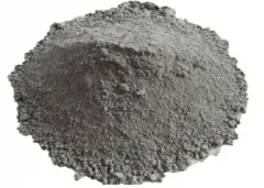
( Silicon Carbide Disc)

Typical Design Applications and Case Studies

In the aerospace area, NASA uses reaction-sintered SiC for the leading side components of the X-43A hypersonic airplane, which can withstand 1700 ° C aerodynamic home heating. GE Aeronautics makes use of HIP-Si two N four to produce generator rotor blades, which is 60% lighter than nickel-based alloys and enables greater operating temperatures. In the clinical field, the crack strength of 3Y-TZP zirconia all-ceramic crowns has actually reached 1400MPa, and the service life can be encompassed greater than 15 years with surface area gradient nano-processing. In the semiconductor industry, high-purity Al two O five ceramics (99.99%) are used as dental caries products for wafer etching tools, and the plasma deterioration rate is <0.1μm/hour. The SiC-Al₂O₃ composite armor developed by Kyocera in Japan can achieve a V50 ballistic limit of 1800m/s, which is 30% thinner than traditional Al₂O₃ armor.

Technical challenges and development trends

The main technical bottlenecks currently faced include: long-term aging of zirconia (strength decay of 30-50% after 10 years), sintering deformation control of large-size SiC ceramics (warpage of > 500mm elements < 0.1 mm ), and high production price of silicon nitride(aerospace-grade HIP-Si five N ₄ reaches $ 2000/kg). The frontier growth instructions are focused on: 1st Bionic structure style(such as shell layered structure to enhance strength by 5 times); ② Ultra-high temperature level sintering modern technology( such as trigger plasma sintering can accomplish densification within 10 mins); three Intelligent self-healing ceramics (including low-temperature eutectic stage can self-heal splits at 800 ° C); four Additive manufacturing technology (photocuring 3D printing precision has gotten to ± 25μm).


( Silicon Nitride Ceramics Tube)

Future growth patterns

In a detailed contrast, alumina will still dominate the standard ceramic market with its price benefit, zirconia is irreplaceable in the biomedical area, silicon carbide is the favored material for severe environments, and silicon nitride has terrific possible in the area of high-end devices. In the following 5-10 years, via the combination of multi-scale architectural policy and smart production innovation, the performance limits of engineering ceramics are expected to achieve brand-new advancements: as an example, the style of nano-layered SiC/C ceramics can attain sturdiness of 15MPa · m 1ST/ TWO, and the thermal conductivity of graphene-modified Al two O six can be enhanced to 65W/m · K. With the improvement of the “twin carbon” method, the application scale of these high-performance ceramics in brand-new power (fuel cell diaphragms, hydrogen storage materials), environment-friendly production (wear-resistant components life raised by 3-5 times) and various other areas is expected to maintain an average annual growth rate of more than 12%.

Supplier

Advanced Ceramics founded on October 17, 2012, is a high-tech enterprise committed to the research and development, production, processing, sales and technical services of ceramic relative materials and products. Our products includes but not limited to Boron Carbide Ceramic Products, Boron Nitride Ceramic Products, Silicon Carbide Ceramic Products, Silicon Nitride Ceramic Products, Zirconium Dioxide Ceramic Products, etc. If you are interested in coated alumina, please feel free to contact us.(nanotrun@yahoo.com)

All articles and pictures are from the Internet. If there are any copyright issues, please contact us in time to delete.

Inquiry us


    The Future is Here: Unleashing the Power of Silicon Carbide onsemi sic mosfet

    Intro to Silicon Carbide

    Silicon carbide, a compound of silicon and carbon, stands apart for its solidity and sturdiness. It finds usage in lots of sectors because of its special homes. This material can manage high temperatures and withstand wear. Its applications vary from electronic devices to vehicle parts. This short article explores the possible and uses silicon carbide.


    (Silicon Carbide Powder)

    Structure and Manufacturing Refine

    Silicon carbide is made by integrating silicon and carbon. These elements are warmed to extremely high temperatures.

    The procedure starts with blending silica sand and carbon in a heater. The mixture is warmed to over 2000 degrees Celsius. At these temperatures, the products react to form silicon carbide crystals. These crystals are after that crushed and arranged by dimension. Various dimensions have different uses. The result is a functional product prepared for numerous applications.

    Applications Across Various Sectors

    Power Electronics

    In power electronics, silicon carbide is utilized in semiconductors. It can take care of greater voltages and operate at higher temperature levels than typical silicon. This makes it suitable for electrical cars and renewable resource systems. Instruments made with silicon carbide are more efficient and smaller sized in size. This saves room and improves efficiency.

    Automotive Sector

    The vehicle sector uses silicon carbide in stopping systems and engine parts. It stands up to wear and heat better than other materials. Silicon carbide brake discs last much longer and perform far better under severe conditions. In engines, it helps reduce rubbing and rise efficiency. This brings about better fuel economic situation and lower exhausts.

    Aerospace and Protection

    In aerospace and protection, silicon carbide is used in shield plating and thermal security systems. It can withstand high impacts and extreme temperature levels. This makes it perfect for safeguarding airplane and spacecraft. Silicon carbide additionally helps in making lightweight yet solid parts. This minimizes weight and enhances payload ability.

    Industrial Uses

    Industries make use of silicon carbide in cutting devices and abrasives. Its hardness makes it excellent for reducing tough materials like steel and stone. Silicon carbide grinding wheels and reducing discs last longer and reduce much faster. This enhances productivity and decreases downtime. Factories also utilize it in refractory cellular linings that secure heating systems and kilns.


    (Silicon Carbide Powder)

    Market Trends and Development Vehicle Drivers: A Progressive Perspective

    Technical Advancements

    New technologies improve just how silicon carbide is made. Much better manufacturing approaches reduced prices and boost top quality. Advanced screening allows makers examine if the materials function as anticipated. This assists produce much better products. Firms that adopt these technologies can use higher-quality silicon carbide.

    Renewable Resource Need

    Growing demand for renewable resource drives the demand for silicon carbide. Photovoltaic panel and wind generators use silicon carbide elements. They make these systems extra reliable and reputable. As the globe changes to cleaner power, using silicon carbide will certainly expand.

    Consumer Understanding

    Customers currently recognize more regarding the advantages of silicon carbide. They look for items that utilize it. Brands that highlight making use of silicon carbide bring in even more customers. Individuals count on products that are more secure and last longer. This fad increases the marketplace for silicon carbide.

    Obstacles and Limitations: Navigating the Path Forward

    Cost Issues

    One difficulty is the price of making silicon carbide. The process can be costly. Nonetheless, the advantages commonly outweigh the costs. Products made with silicon carbide last longer and perform much better. Business should show the value of silicon carbide to justify the rate. Education and advertising can assist.

    Safety and security Issues

    Some worry about the safety of silicon carbide. Dirt from cutting or grinding can trigger wellness concerns. Study is recurring to make certain secure handling techniques. Rules and standards aid regulate its use. Business must follow these rules to shield workers. Clear communication about safety can construct trust.

    Future Potential Customers: Advancements and Opportunities

    The future of silicon carbide looks appealing. Extra study will find brand-new ways to utilize it. Innovations in products and technology will certainly improve its efficiency. As sectors seek better remedies, silicon carbide will certainly play an essential role. Its capability to manage high temperatures and resist wear makes it beneficial. The constant development of silicon carbide assures amazing possibilities for growth.

    Provider

    TRUNNANO is a supplier of Silicon Carbide with over 12 years experience in nano-building energy conservation and nanotechnology development. It accepts payment via Credit Card, T/T, West Union and Paypal. Trunnano will ship the goods to customers overseas through FedEx, DHL, by air, or by sea. If you want to know more about Silicon Carbide, please feel free to contact us and send an inquiry.(sales5@nanotrun.com)
    Tags: silicon carbide,silicon carbide mosfet,mosfet sic

    All articles and pictures are from the Internet. If there are any copyright issues, please contact us in time to delete.

    Inquiry us


      Silicon Dioxide: The Backbone of Modern Innovation and Sustainability na2o al2o3 sio2

      Introduction to Silicon Dioxide (SiO ₂)

      Silicon dioxide, generally known as silica and with the compound name SiO ₂, is one of one of the most plentiful compounds in the world. Found in various kinds such as quartz, sand, and glass, silicon dioxide plays a critical function in countless industries, from construction to electronics. This short article explores the make-up, properties, applications, and future prospects of silicon dioxide, highlighting its transformative impact on modern-day innovation and market.


      (Nano Silicon Dioxide)

      The Chemical Structure and Residence of Silicon Dioxide

      Silicon dioxide has the chemical formula SiO ₂, including one silicon atom bound to two oxygen atoms. This structure presents a number of remarkable residential properties, including high thermal security, superb protecting capabilities, and resistance to chemical attack. Silicon dioxide exists in several crystalline forms, with quartz being the most typical. These forms show one-of-a-kind physical and chemical characteristics, making silicon dioxide functional for diverse applications. Its capability to form steady bonds and resist destruction under extreme problems positions it as an essential product in advanced manufacturing processes.

      Applications Throughout Various Sectors

      1. Building And Construction and Building Products: In building, silicon dioxide is a main element of concrete, blocks, and glass. Its durability and stamina enhance the structural stability of buildings, guaranteeing long-lasting performance. Silica-based materials supply outstanding thermal insulation, lowering energy intake and boosting sustainability. Additionally, silicon dioxide’s capacity to bond snugly with other materials makes it essential in mortar and concrete formulas. The use of silica in building and construction not only enhances constructing top quality but additionally promotes environmental responsibility through reduced maintenance and longer life-spans.

      2. Electronic devices and Semiconductors: Silicon dioxide plays an essential duty in the electronic devices market, especially in semiconductor production. As an insulator, it creates the gate oxide layer in transistors, protecting against electrical leakage and ensuring efficient procedure. High-purity silicon dioxide is made use of in integrated circuits, solar batteries, and fiber optics, where its openness and dielectric homes are crucial. Developments in nanotechnology have actually additionally expanded silicon dioxide’s applications, making it possible for the development of smaller, much faster, and more reliable electronic gadgets. The integration of silicon dioxide in advanced technologies highlights its significance in driving innovation and performance.

      3. Medical care and Pharmaceuticals: In medical care, silicon dioxide serves as an excipient in pharmaceutical formulations, enhancing drug delivery and security. It serves as a glidant, enhancing powder flowability throughout tablet manufacturing, and as an anti-caking representative, avoiding jumble. Silica nanoparticles are likewise utilized in targeted medication delivery systems, supplying precise control over launch rates and enhancing healing results. Additionally, silicon dioxide’s biocompatibility makes it appropriate for clinical implants and diagnostic tools, ensuring person security and efficacy. The adaptability of silicon dioxide in health care applications highlights its potential to reinvent clinical treatments and client treatment.

      4. Cosmetics and Personal Care Products: Silicon dioxide discovers extensive use in cosmetics and individual care products, where it supplies structure, absorbency, and sensory advantages. Silica powders improve the spreadability and surface of make-up, skincare, and hair products, improving consumer satisfaction. Its non-toxic nature and capacity to soak up excess oils make it optimal for solutions targeting oily skin and hair. Furthermore, silicon dioxide’s UV-blocking properties offer security versus harmful sunlight rays, adding to skin wellness and charm. The cosmetic market’s concentrate on natural and useful active ingredients positions silicon dioxide as a recommended selection for cutting-edge product advancement.

      Market Patterns and Growth Drivers: A Forward-Looking Viewpoint

      1. Sustainability Campaigns: The international push for sustainable methods has pushed silicon dioxide into the spotlight. Originated from abundant natural deposits, silicon dioxide lines up well with environmentally friendly construction and manufacturing criteria. Makers increasingly incorporate silicon dioxide right into green building materials and renewable resource technologies, driving market development. Developments in recycling and resource-efficient manufacturing techniques additionally improve silicon dioxide’s sustainability account. As environmental recognition grows, the fostering of silicon dioxide will certainly continue to raise, positioning it as a key player in lasting remedies.

      2. Technical Improvements in Electronic Devices: Quick developments in electronic devices demand higher-performance materials efficient in conference rigid demands. Silicon dioxide’s duty in semiconductor fabrication guarantees its significance in next-generation modern technologies. Innovations in 5G networks, expert system, and quantum computer rely upon silicon dioxide’s protecting and dielectric residential or commercial properties to attain ideal performance. The integration of silicon dioxide in these sophisticated applications showcases its flexibility and future-proof nature. As electronics progress, silicon dioxide stays at the leading edge of technological development.

      3. Health Care Advancement: Climbing medical care expense, driven by maturing populations and raised wellness recognition, boosts the need for advanced clinical options. Silicon dioxide’s multifunctional residential properties make it an attractive element in medicine distribution systems, medical tools, and diagnostics. The fad towards personalized medicine and minimally intrusive therapies prefers silicon dioxide’s biocompatibility and accuracy. As medical care continues to prioritize advancement and patient-centric solutions, silicon dioxide’s duty in advancing clinical innovations can not be overemphasized.

      Difficulties and Limitations: Browsing the Path Forward

      1. Environmental Worries: Despite its advantages, the mining and processing of silicon dioxide can have ecological effects. Dust discharges and water usage throughout removal raising worries regarding air quality and source depletion. Regulatory bodies are applying stricter standards to alleviate these impacts, prompting suppliers to embrace lasting practices. Resolving ecological obstacles will be critical for the proceeded use and market approval of silicon dioxide. Technologies in eco-friendly chemistry and procedure optimization can help stabilize efficiency with ecological responsibility.

      2. Technical Expertise: Efficiently incorporating silicon dioxide right into formulas requires specialized understanding and handling strategies. Small-scale manufacturers or those unfamiliar with its buildings could face challenges in enhancing silicon dioxide use without appropriate competence and devices. Bridging this gap with education and obtainable innovation will be important for more comprehensive adoption. Encouraging stakeholders with the required skills will open silicon dioxide’s complete potential throughout sectors.


      (Nano Silicon Dioxide)

      Future Prospects: Technologies and Opportunities

      The future of the silicon dioxide market looks appealing, driven by boosting need for sustainable and high-performance materials. Continuous research and development will result in the development of brand-new grades and applications for silicon dioxide. Innovations in nanotechnology, naturally degradable materials, and green chemistry will additionally enhance its worth recommendation. As industries prioritize performance, resilience, and environmental duty, silicon dioxide is poised to play a crucial function in shaping the future of construction, electronic devices, health care, and beyond. The constant evolution of silicon dioxide guarantees interesting opportunities for development and development.

      Conclusion: Welcoming the Potential of Silicon Dioxide

      In conclusion, silicon dioxide (SiO ₂) is a versatile and important compound with comprehensive applications in construction, electronics, healthcare, and cosmetics. Its distinct residential or commercial properties and bountiful availability offer significant benefits, driving market development and advancement. Understanding the advantages and difficulties of silicon dioxide enables stakeholders to make educated decisions and maximize arising possibilities. Accepting silicon dioxide indicates welcoming a future where development meets integrity and sustainability in modern sector.

      Top Notch Silicon Dioxide Distributor

      TRUNNANO is a supplier of nano materials with over 12 years experience in nano-building energy conservation and nanotechnology development. It accepts payment via Credit Card, T/T, West Union and Paypal. Trunnano will ship the goods to customers overseas through FedEx, DHL, by air, or by sea. If you want to know more about Nano Silicon Dioxide, please feel free to contact us and send an inquiry.(sales5@nanotrun.com)

      All articles and pictures are from the Internet. If there are any copyright issues, please contact us in time to delete.

      Inquiry us


        In-depth Analysis of Nano Silicon Dioxide (Nano SiO2): A Comprehensive Exploration from Basics to Applications sio2 amorphous

        Extensive Analysis of Nano Silicon Dioxide (Nano SiO2): An Extensive Exploration from Basics to Applications

        As technology advancements and commercial demands increase, nanomaterials have ended up being a centerpiece in modern-day materials science throughout various areas. Nano silicon dioxide (Nano SiO2), as a result of its one-of-a-kind physical and chemical residential or commercial properties, has shown impressive potential in numerous applications. It refers to silica fragments with dimensions varying from 1 to 100 nanometers. Compared to standard micron-sized silica, nano SiO2 shows greater specific surface area, better surface energy, and premium optical, electric, and mechanical buildings. These functions grant it with extensive application worth in areas such as catalyst carriers, adsorbents, finishing products, electronic devices, and biomedicine. Additionally, nano SiO2 reveals superb chemical and thermal stability, maintaining its framework and function under extreme problems. As an example, in the electronic devices market, nano SiO2 is made use of as a shielding layer and passivation layer to make certain circuit stability; it is also an optimal choice for lithium-ion battery anode materials. In biomedicine, nano SiO2 bits can be made use of for targeted medication delivery systems and as cell pens or fluorescent probes to assist illness diagnosis.


        (Nano Silicon Dioxide)

        The prep work strategies for nano SiO2 vary and include sol-gel methods, rainfall techniques, vapor deposition methods, to name a few. Each technique has its features and applicability. The sol-gel method entails progressively transforming forerunner solutions right into gels, complied with by drying and calcination to acquire nano SiO2 powders. This approach is easy to operate and permits specific control over the morphology and particle size distribution of the product. Rainfall techniques make use of acid-base responses or complexation responses to produce hydroxide speeds up, which are then dehydrated to form nano SiO2. This technique is economical and suitable for large-scale manufacturing. Vapor deposition techniques, including physical vapor deposition (PVD) and chemical vapor deposition (CVD), are suitable for preparing premium, high-purity nano films or powders. Over the last few years, new prep work technologies like microemulsion approaches and supercritical fluid innovation have actually been created, providing more possibilities for tailored synthesis of nano SiO2. In China, with rapid economic growth and technical improvements, the nano SiO2 market has actually revealed durable development. According to relevant statistics, China’s nano SiO2 market dimension surpassed RMB 10 billion in 2023 and is anticipated to preserve high development prices in the coming years. This mirrors the solid residential demand and enhanced assistance for the brand-new materials industry.

        Leveraging its extraordinary performance, nano SiO2 discovers prevalent applications in construction materials, electronic devices, biomedicine, ecological administration, and beyond. In building materials, nano SiO2 as a high-performance concrete additive considerably enhances concrete strength, durability, and water resistance; when related to glass surface area alteration, it boosts light transmission and self-cleaning capability. In the electronic devices industry, it works as an optimal shielding layer and passivation layer during semiconductor production and is likewise a recommended material for lithium-ion battery anodes. In biomedicine, nano SiO2 fragments make it possible for targeted medicine shipment and function as cell pens and fluorescent probes for disease medical diagnosis. In environmental management, because of its effective adsorption and catalytic task, nano SiO2 is extensively used in wastewater treatment and air filtration, helping get rid of hazardous materials and enhance ecological high quality. In addition, nano SiO2 has located a location in cosmetics and personal treatment products, such as functioning as UV shielding representatives in sunscreens, supplying highly effective security. Its multifunctional nature makes nano SiO2 an essential material for cross-industry innovation.


        (Nano Silicon Dioxide)

        Looking ahead, nano SiO2 will accomplish considerable progress in intelligent applications, green sustainable advancement, and interdisciplinary collaboration. Leveraging advanced technologies like the Internet of Things (IoT) and big information analytics, nano SiO2 can be deeply integrated right into smart structures and wise homes, using easier and comfy living experiences. Developing eco-friendly preparation procedures reduces power consumption and waste exhausts, promoting a transition in the direction of low-carbon, round growth. Strengthening interdisciplinary cooperation to tackle vital technical bottlenecks will advertise ingenious applications of nano SiO2 in emerging fields. For example, combining nanotechnology with artificial intelligence can create self-healing wise materials, further improving product sturdiness and safety. Additionally, attending to the possible security and wellness risks associated with nanomaterials, international requirements and guidelines have actually been developed to guide their risk-free administration and evaluation. In recap, encountering transforming market needs and technological difficulties, just continuous technology can keep pace with this age full of chances. We believe that in the near future, we will witness much more impressive technological accomplishments in this field, contributing to producing a much better living setting for humanity. As international interest shifts towards sustainable development, research and applications of nano SiO2 will continue to broaden, supplying new ideas and services to deal with ecological problems and societal needs.

        TRUNNANO is a supplier of nano materials with over 12 years experience in nano-building energy conservation and nanotechnology development. It accepts payment via Credit Card, T/T, West Union and Paypal. Trunnano will ship the goods to customers overseas through FedEx, DHL, by air, or by sea. If you want to know more about Nano Silicon Dioxide, please feel free to contact us and send an inquiry.(sales5@nanotrun.com)

        All articles and pictures are from the Internet. If there are any copyright issues, please contact us in time to delete.

        Inquiry us


          Nano-Silica: A New Generation of Multi-functional Materials Leading the Revolution in Material Science periodic table silicon

          Nano-Silica: A New Generation of Multi-functional Materials Leading the Revolution in Product Scientific Research

          Nano-silica (Nano-Silica), as a sophisticated product with one-of-a-kind physical and chemical homes, has actually demonstrated substantial application capacity throughout many areas over the last few years. It not only acquires the standard attributes of traditional silica, such as high solidity, excellent thermal security, and chemical inertness, however additionally exhibits unique properties due to its ultra-fine dimension result. These include a big details surface area, quantum dimension effects, and boosted surface area task. The large details area significantly enhances adsorption capacity and catalytic task, while the quantum size impact modifies optical and electric homes as fragment size lowers. The increased proportion of surface area atoms results in stronger sensitivity and selectivity.

          Presently, preparing high-grade nano-silica employs several methods: Sol-Gel Process: Via hydrolysis and condensation responses, this approach changes silicon ester forerunners right into gel-like substances, which are then dried and calcined to produce final products. This technique permits precise control over morphology and particle dimension distribution, suitable for bulk production. Rainfall Technique: By readjusting the pH value of solutions, SiO ₂ can precipitate out under specific problems. This technique is straightforward and cost-effective. Vapor Deposition Approaches (PVD/CVD): Appropriate for developing thin movies or composite materials, these methods entail transferring silicon dioxide from the vapor phase. Microemulsion Technique: Using surfactants to form micro-sized oil-water interfaces as themes, this approach promotes the synthesis of uniformly spread nanoparticles under mild problems.


          (Nano Silicon Dioxide)

          These innovative synthesis modern technologies offer a robust structure for exploring the potential applications of nano-silica in numerous circumstances.

          In recent times, researchers have uncovered that nano-silica master multiple areas: Efficient Stimulant Carriers: With plentiful pore structures and flexible surface functional groups, nano-silica can properly fill metal nanoparticles or other active species, locating wide applications in petrochemicals and great chemicals. Exceptional Reinforcing Fillers: As a suitable strengthening agent, nano-silica can substantially boost the mechanical stamina, put on resistance, and warmth resistance of polymer-based composites, such as in tire manufacturing to improve traction and fuel performance. Excellent Finishing Materials: Leveraging its superior transparency and weather condition resistance, nano-silica is commonly used in layers, paints, and glass plating to offer far better protective performance and visual end results. Smart Drug Shipment Systems: Nano-silica can be changed to introduce targeting particles or receptive groups, allowing selective shipment to details cells or tissues, ending up being a research focus in cancer cells therapy and other medical fields.

          These study findings have actually greatly driven the transition of nano-silica from research laboratory setups to industrial applications. Globally, many countries and areas have actually enhanced financial investment in this field, intending to develop more affordable and useful services and products.

          Nano-silica’s applications showcase its considerable possible across various industries: New Power Lorry Batteries: In the global new energy automobile market, attending to high battery costs and short driving arrays is vital. Nano-silica acts as an unique additive in lithium-ion batteries, where it boosts electrode conductivity and architectural security, inhibits side responses, and extends cycle life. As an example, Tesla includes nano-silica right into nickel-cobalt-aluminum (NCA) cathode products, substantially enhancing the Model 3’s range. High-Performance Structure Products: The building market looks for energy-saving and environmentally friendly materials. Nano-silica can be utilized as an admixture in cement concrete, loading internal spaces and maximizing microstructure to boost compressive stamina and longevity. In addition, nano-silica self-cleaning layers put on exterior walls decompose air contaminants and stop dirt buildup, preserving building appearances. Research study at the Ningbo Institute of Products Innovation and Design, Chinese Academy of Sciences, reveals that nano-silica-enhanced concrete does excellently in freeze-thaw cycles, remaining undamaged also after several temperature level modifications. Biomedical Diagnosis and Treatment: As health recognition expands, nanotechnology’s function in biomedical applications increases. Due to its excellent biocompatibility and simplicity of alteration, nano-silica is perfect for constructing clever diagnostic platforms. For instance, researchers have designed a detection technique utilizing fluorescently labeled nano-silica probes to swiftly determine cancer cells cell-specific markers in blood samples, using greater sensitivity than typical techniques. During illness treatment, drug-loaded nano-silica pills launch medicine based upon ecological adjustments within the body, exactly targeting affected locations to lower side effects and boost effectiveness. Stanford University School of Medicine efficiently established a temperature-sensitive drug distribution system made up of nano-silica, which immediately initiates medication release at body temperature level, efficiently intervening in breast cancer cells therapy.


          (Nano Silicon Dioxide)

          Despite the substantial success of nano-silica materials and associated modern technologies, obstacles remain in sensible promo and application: Price Issues: Although basic materials for nano-silica are relatively affordable, intricate preparation processes and specific tools lead to higher total item prices, affecting market competition. Large-Scale Manufacturing Innovation: The majority of existing synthesis approaches are still in the speculative stage, lacking mature commercial production procedures to satisfy large market demands. Ecological Friendliness: Some preparation procedures may produce dangerous byproducts, necessitating further optimization to guarantee eco-friendly manufacturing practices. Standardization: The lack of merged item specifications and technical criteria results in irregular high quality among products from different producers, making complex customer choices.

          To overcome these challenges, continuous development and improved collaboration are necessary. On one hand, deepening fundamental study to discover brand-new synthesis approaches and enhance existing procedures can continuously minimize manufacturing costs. On the other hand, developing and refining sector requirements promotes worked with growth among upstream and downstream enterprises, constructing a healthy and balanced environment. Colleges and study institutes must raise educational financial investments to cultivate more high-grade specialized skills, laying a solid skill foundation for the lasting growth of the nano-silica market.

          In recap, nano-silica, as a highly appealing multi-functional material, is slowly changing numerous aspects of our lives. From new energy vehicles to high-performance building materials, from biomedical diagnostics to smart medication delivery systems, its visibility is common. With continuous technological maturation and perfection, nano-silica is expected to play an irreplaceable function in extra areas, bringing better comfort and advantages to human society in the coming years.

          TRUNNANO is a supplier of Nano Silicon Dioxide with over 12 years experience in nano-building energy conservation and nanotechnology development. It accepts payment via Credit Card, T/T, West Union and Paypal. Trunnano will ship the goods to customers overseas through FedEx, DHL, by air, or by sea. If you want to know more about Nano Silicon Dioxide, please feel free to contact us and send an inquiry.(sales5@nanotrun.com)

          All articles and pictures are from the Internet. If there are any copyright issues, please contact us in time to delete.

          Inquiry us


            Silicon Carbide: Leading the Revolution in Semiconductor Materials with Advanced Power Devices sic wafer cost

            Silicon Carbide: Leading the Transformation in Semiconductor Products with Advanced Power Tools

            Silicon carbide (SiC), as a representative of third-generation wide-bandgap semiconductor materials, showcases immense application potential across power electronic devices, brand-new energy vehicles, high-speed trains, and other fields due to its remarkable physical and chemical buildings. It is a substance composed of silicon (Si) and carbon (C), including either a hexagonal wurtzite or cubic zinc mix structure. SiC flaunts an extremely high failure electrical field strength (roughly 10 times that of silicon), reduced on-resistance, high thermal conductivity (3.3 W/cm · K compared to silicon’s 1.5 W/cm · K), and high-temperature resistance (up to above 600 ° C). These qualities allow SiC-based power tools to run stably under greater voltage, frequency, and temperature level conditions, accomplishing much more reliable power conversion while substantially decreasing system dimension and weight. Particularly, SiC MOSFETs, contrasted to traditional silicon-based IGBTs, use faster changing speeds, reduced losses, and can stand up to greater present densities; SiC Schottky diodes are extensively used in high-frequency rectifier circuits due to their zero reverse healing attributes, properly minimizing electro-magnetic interference and power loss.


            (Silicon Carbide Powder)

            Because the effective prep work of top quality single-crystal SiC substrates in the early 1980s, researchers have actually gotten rid of many crucial technical difficulties, consisting of premium single-crystal growth, problem control, epitaxial layer deposition, and processing methods, driving the development of the SiC industry. Internationally, several firms focusing on SiC product and gadget R&D have emerged, such as Wolfspeed (previously Cree) from the U.S., Rohm Co., Ltd. from Japan, and Infineon Technologies AG from Germany. These firms not only master innovative production modern technologies and patents but additionally proactively participate in standard-setting and market promotion tasks, promoting the continuous renovation and development of the whole commercial chain. In China, the government positions substantial focus on the ingenious capabilities of the semiconductor industry, presenting a collection of supportive plans to motivate ventures and research organizations to raise financial investment in arising fields like SiC. By the end of 2023, China’s SiC market had exceeded a scale of 10 billion yuan, with assumptions of ongoing quick development in the coming years. Recently, the global SiC market has seen several vital innovations, including the effective development of 8-inch SiC wafers, market need growth forecasts, policy assistance, and participation and merger events within the market.

            Silicon carbide shows its technological benefits via numerous application instances. In the new energy lorry market, Tesla’s Model 3 was the initial to embrace complete SiC modules as opposed to traditional silicon-based IGBTs, enhancing inverter efficiency to 97%, boosting acceleration performance, decreasing cooling system concern, and extending driving array. For photovoltaic power generation systems, SiC inverters much better adjust to complicated grid settings, demonstrating stronger anti-interference abilities and vibrant response rates, particularly excelling in high-temperature problems. According to estimations, if all freshly included solar setups across the country taken on SiC modern technology, it would certainly save 10s of billions of yuan annually in electrical energy costs. In order to high-speed train grip power supply, the most up to date Fuxing bullet trains include some SiC parts, attaining smoother and faster beginnings and decelerations, boosting system integrity and upkeep benefit. These application instances highlight the massive capacity of SiC in improving performance, decreasing expenses, and boosting reliability.


            (Silicon Carbide Powder)

            Regardless of the many advantages of SiC products and devices, there are still obstacles in useful application and promotion, such as expense problems, standardization building, and skill farming. To gradually get rid of these challenges, industry professionals believe it is essential to innovate and enhance participation for a brighter future continually. On the one hand, growing fundamental study, checking out new synthesis approaches, and enhancing existing processes are necessary to continually lower manufacturing costs. On the other hand, establishing and improving market standards is crucial for advertising collaborated development among upstream and downstream business and constructing a healthy and balanced ecosystem. In addition, colleges and study institutes ought to increase instructional investments to cultivate more premium specialized skills.

            Overall, silicon carbide, as a highly appealing semiconductor product, is slowly changing different elements of our lives– from new power cars to wise grids, from high-speed trains to commercial automation. Its presence is common. With recurring technical maturity and excellence, SiC is expected to play an irreplaceable duty in numerous areas, bringing more comfort and benefits to human society in the coming years.

            TRUNNANO is a supplier of Silicon Carbide with over 12 years experience in nano-building energy conservation and nanotechnology development. It accepts payment via Credit Card, T/T, West Union and Paypal. Trunnano will ship the goods to customers overseas through FedEx, DHL, by air, or by sea. If you want to know more about Silicon Carbide, please feel free to contact us and send an inquiry.(sales5@nanotrun.com)

            All articles and pictures are from the Internet. If there are any copyright issues, please contact us in time to delete.

            Inquiry us


              Silicon Carbide: Leading the Revolution in Semiconductor Materials with Advanced Power Devices sanan sic

              Silicon Carbide: Leading the Change in Semiconductor Materials with Advanced Power Gadget

              Carbonized silicon (Silicon Carbide, SiC), as an agent of third-generation wide-bandgap semiconductor products, has shown enormous application potential against the backdrop of growing international demand for tidy power and high-efficiency electronic tools. Silicon carbide is a compound made up of silicon (Si) and carbon (C), featuring either a hexagonal wurtzite or cubic zinc mix framework. It boasts remarkable physical and chemical residential or commercial properties, consisting of an exceptionally high malfunction electrical field strength (about 10 times that of silicon), reduced on-resistance, high thermal conductivity (3.3 W/cm · K contrasted to silicon’s 1.5 W/cm · K), and high-temperature resistance (up to over 600 ° C). These features permit SiC-based power tools to run stably under higher voltage, frequency, and temperature conditions, accomplishing more effective power conversion while dramatically reducing system size and weight. Especially, SiC MOSFETs, compared to conventional silicon-based IGBTs, provide faster changing rates, lower losses, and can endure better existing densities, making them perfect for applications like electrical lorry charging stations and solar inverters. At The Same Time, SiC Schottky diodes are extensively made use of in high-frequency rectifier circuits as a result of their absolutely no reverse recovery characteristics, successfully reducing electro-magnetic interference and energy loss.


              (Silicon Carbide Powder)

              Because the effective prep work of premium single-crystal silicon carbide substratums in the very early 1980s, scientists have conquered various crucial technical difficulties, such as high-grade single-crystal development, defect control, epitaxial layer deposition, and handling techniques, driving the advancement of the SiC sector. Worldwide, numerous business focusing on SiC product and gadget R&D have arised, consisting of Cree Inc. from the United State, Rohm Co., Ltd. from Japan, and Infineon Technologies AG from Germany. These companies not just master sophisticated manufacturing innovations and patents however additionally actively take part in standard-setting and market promo activities, promoting the continuous improvement and development of the whole industrial chain. In China, the federal government positions substantial focus on the ingenious abilities of the semiconductor industry, introducing a collection of helpful plans to encourage ventures and study organizations to raise financial investment in emerging fields like SiC. By the end of 2023, China’s SiC market had actually exceeded a range of 10 billion yuan, with assumptions of ongoing quick growth in the coming years.

              Silicon carbide showcases its technical advantages with numerous application instances. In the brand-new power automobile market, Tesla’s Version 3 was the first to take on complete SiC modules instead of standard silicon-based IGBTs, improving inverter effectiveness to 97%, enhancing velocity performance, lowering cooling system concern, and extending driving range. For solar power generation systems, SiC inverters much better adjust to complicated grid atmospheres, demonstrating stronger anti-interference abilities and dynamic response rates, specifically mastering high-temperature problems. In terms of high-speed train traction power supply, the latest Fuxing bullet trains include some SiC parts, accomplishing smoother and faster begins and slowdowns, enhancing system dependability and upkeep benefit. These application instances highlight the massive potential of SiC in enhancing performance, minimizing expenses, and improving integrity.


              ()

              Regardless of the lots of advantages of SiC products and gadgets, there are still difficulties in sensible application and promotion, such as price problems, standardization construction, and skill growing. To progressively overcome these barriers, industry specialists think it is needed to innovate and enhance collaboration for a brighter future continually. On the one hand, growing basic research, exploring brand-new synthesis methods, and enhancing existing procedures are necessary to constantly lower production costs. On the other hand, establishing and improving sector criteria is crucial for promoting coordinated development among upstream and downstream business and developing a healthy ecosystem. Moreover, universities and research study institutes must raise instructional financial investments to cultivate more high-quality specialized skills.

              In summary, silicon carbide, as an extremely encouraging semiconductor material, is progressively changing different facets of our lives– from brand-new power vehicles to wise grids, from high-speed trains to industrial automation. Its existence is common. With recurring technological maturation and excellence, SiC is expected to play an irreplaceable duty in a lot more fields, bringing even more ease and advantages to culture in the coming years.

              TRUNNANO is a supplier of Silicon Carbide with over 12 years of experience in nano-building energy conservation and nanotechnology development. It accepts payment via Credit Card, T/T, West Union and Paypal. Trunnano will ship the goods to customers overseas through FedEx, DHL, by air, or by sea. If you want to know more about Silicon Carbide, please feel free to contact us and send an inquiry(sales8@nanotrun.com).

              All articles and pictures are from the Internet. If there are any copyright issues, please contact us in time to delete.

              Inquiry us


                Silicon Hexaboride Market Report and Outlook (2025-2030) sib 15

                We Offer Silicon Hexaboride Specifications

                Our Silicon Hexaboride (SiB6) is a glossy black-gray powder defined by its high pureness exceeding 99%. With a relative density of 3.0 g/cm3 and a melting point of 2200 ° C, it makes certain phenomenal performance in high-temperature applications. The bit dimension varies in between 20-40 micrometers, making it appropriate for numerous industrial usages needing accuracy and harmony. Get in touch with us for comprehensive specs and inquiries concerning our Silicon Hexaboride.


                (TRUNNANO Silicon Hexaboride)

                Introduction

                The global Silicon Hexaboride (SiB6) market is poised for considerable growth from 2025 to 2030. SiB6 is a substance with impressive residential or commercial properties, consisting of high solidity, thermal stability, and chemical inertness. These qualities make it very beneficial in different markets, such as electronics, aerospace, and advanced products. This record gives a comprehensive overview of the present market condition, crucial drivers, difficulties, and future potential customers.

                Market Overview

                Silicon Hexaboride is primarily utilized in the manufacturing of advanced porcelains, abrasives, and refractory materials. Its high hardness and put on resistance make it ideal for applications in cutting tools, grinding wheels, and wear-resistant coatings. In the electronic devices industry, SiB6 is made use of in the fabrication of semiconductor gadgets and as a safety finishing due to its outstanding thermal and chemical security. The marketplace is segmented by type, application, and area, each adding to the overall market characteristics.

                Secret Drivers

                One of the key motorists of the SiB6 market is the increasing demand for sophisticated ceramics in the aerospace and vehicle industries. SiB6’s high solidity and put on resistance make it a recommended material for making parts that run under extreme problems. In addition, the growing use of SiB6 in the manufacturing of abrasives and refractory materials is driving market development. The electronic devices market’s demand for products with high thermal and chemical security is one more significant driver.

                Difficulties

                In spite of its many advantages, the SiB6 market encounters numerous obstacles. One of the major difficulties is the high price of production, which can limit its prevalent fostering in cost-sensitive applications. The complicated production procedure, consisting of synthesis and sintering, requires substantial capital investment and technical experience. Environmental problems connected to the removal and handling of silicon and boron are likewise important factors to consider. Ensuring sustainable and eco-friendly production methods is essential for the long-term development of the marketplace.

                Technical Advancements

                Technical developments play a crucial function in the growth of the SiB6 market. Technologies in synthesis techniques, such as hot pressing and trigger plasma sintering (SPS), have enhanced the top quality and uniformity of SiB6 items. These strategies permit specific control over the microstructure and homes of SiB6, allowing its usage in more requiring applications. Research and development efforts are additionally focused on creating composite materials that incorporate SiB6 with other materials to enhance their performance and expand their application range.

                Regional Analysis

                The global SiB6 market is geographically varied, with North America, Europe, Asia-Pacific, and the Center East & Africa being vital areas. North America and Europe are expected to maintain a solid market presence as a result of their sophisticated production markets and high demand for high-performance materials. The Asia-Pacific region, particularly China and Japan, is projected to experience substantial growth because of rapid industrialization and increasing financial investments in r & d. The Center East and Africa, while currently smaller sized markets, show potential for development driven by framework growth and arising sectors.

                Competitive Landscape

                The SiB6 market is very competitive, with numerous well established gamers controling the market. Key players consist of companies such as H.C. Starck, Alfa Aesar, and Advanced Ceramics Corporation. These firms are continuously purchasing R&D to create cutting-edge products and broaden their market share. Strategic collaborations, mergings, and procurements are common approaches employed by these firms to remain ahead in the market. New entrants deal with challenges due to the high first financial investment required and the need for sophisticated technical abilities.


                ( TRUNNANO Silicon Hexaboride )

                Future Prospects

                The future of the SiB6 market looks appealing, with numerous elements anticipated to drive development over the following 5 years. The boosting concentrate on sustainable and reliable production processes will certainly produce brand-new opportunities for SiB6 in numerous industries. Additionally, the advancement of new applications, such as in additive production and biomedical implants, is anticipated to open brand-new opportunities for market expansion. Federal governments and personal organizations are likewise purchasing study to discover the complete potential of SiB6, which will certainly further add to market development.

                Final thought

                Finally, the worldwide Silicon Hexaboride market is readied to expand substantially from 2025 to 2030, driven by its special buildings and broadening applications throughout several sectors. Regardless of encountering some obstacles, the market is well-positioned for long-term success, supported by technical developments and tactical campaigns from principals. As the demand for high-performance products remains to climb, the SiB6 market is expected to play a crucial function in shaping the future of production and modern technology.

                TRUNNANO is a supplier of Silicon Hexaboride with over 12 years of experience in nano-building energy conservation and nanotechnology development. It accepts payment via Credit Card, T/T, West Union and Paypal. Trunnano will ship the goods to customers overseas through FedEx, DHL, by air, or by sea. If you want to know more about sib 15, please feel free to contact us and send an inquiry(sales5@nanotrun.com).

                All articles and pictures are from the Internet. If there are any copyright issues, please contact us in time to delete.

                Inquiry us


                  Silicon Carbide Market Report and Outlook (2025-2030) mymanmitt.com

                  We Offer Different Requirements of Silicon Carbide

                  We provide a series of Silicon Carbide (SiC) specifications, from ultrafine particles of 60nm to whisker types, covering a large range of bit dimensions. Each specification keeps a high pureness level of SiC, usually ≥ 97% for the tiniest dimension and ≥ 99% for others. The crystalline phase differs depending on the fragment size, with β-SiC predominant in finer sizes and α-SiC appearing in larger dimensions. We ensure very little impurities, with Fe ₂ O ₃ content ≤ 0.13% for the finest grade and ≤ 0.03% for all others, F.C. ≤ 0.8%, F.Si ≤ 0.69%, and total oxygen (T.O.)

                  TRUNNANO is a supplier of silicon carbide with over 12 years of experience in nano-building energy conservation and nanotechnology development. It accepts payment via Credit Card, T/T, West Union and Paypal. Trunnano will ship the goods to customers overseas through FedEx, DHL, by air, or by sea. If you want to know more about mymanmitt.com, please feel free to contact us and send an inquiry(sales5@nanotrun.com).

                  All articles and pictures are from the Internet. If there are any copyright issues, please contact us in time to delete.

                  Inquiry us


                    Global Silicon Nitride Market Overview si3n4 bearing

                    Requirements of Silicon Nitride Si3N4 Powder

                    Product Call: Silicon Nitride


                    (TRUNNANO Silicon Nitride)

                    Pureness: 99%

                    Silicon nitride powders are readily available in two primary types based upon their crystal framework: α-Si3N4 and β-Si3N4. Each form supplies various purities and fragment dimensions to fit various applications.

                    For the α-Si3N4 phase, the greatest purity readily available is 99.995%, with fragment dimensions varying from 1-3 μm, 3-5 μm, 5-10 μm, and 10-15 μm. There is likewise a choice with a pureness of 99.9%, which supplies finer bit sizes, consisting of 0.5-1 μm, 1-3 μm, 3-5 μm, and 5-10 μm.

                    The β-Si3N4 stage is used with pureness of 99.9% and 99.8%, and fragment dimensions include 1-2 μm, 3-5 μm, 10 μm, 10-15 μm, and 15-20 μm. Additionally, there is a β-Si3N4 choice with a purity more than 95%, offered in particle dimensions of 1-3 μm and 3-5 μm.

                    In summary, our range of silicon nitride powders supplies a broad selection of pureness and bit dimensions, dealing with varied application demands. Whether high purity or specific fragment dimension is needed, suitable choices can be discovered within our product offerings.

                    Silicon nitride (Si3N4) is a high-performance ceramic material known for its exceptional thermal and mechanical properties. Its remarkable strength, reduced thermal expansion, and superior wear resistance have made it a favored choice in sectors such as automotive, electronic devices, and aerospace. These characteristics have promoted its wide adoption throughout various markets.

                    Market Drivers

                    The silicon nitride market’s development is largely driven by technical advancements and the increasing demand for products that can stand up to severe conditions. In the auto market, silicon nitride is used in engine parts to boost fuel effectiveness and minimize car weight. In the electronic devices industry, it works as a protecting layer in semiconductors, assisting in the miniaturization and performance improvement of digital tools. In spite of the high production expenses and intricate manufacturing procedures, continuous r & d initiatives are concentrated on maximizing production methods, reducing expenses, and expanding market reach.

                    Regional Analysis

                    The Asia-Pacific area leads the international silicon nitride market, driven by its strong industrial base and the presence of crucial producers in nations like China, Japan, and South Korea. These areas go to the forefront of technological development, which enhances the demand for advanced materials like silicon nitride. Europe and North America also hold considerable market shares, particularly in aerospace and defense applications. The Center East and Africa, while smaller sized markets, reveal potential, specifically in the oil and gas market, where the material’s sturdiness and put on resistance are highly valued.


                    ( TRUNNANO Silicon Nitride )

                    Future Outlook

                    The silicon nitride market is expected to see significant development in the coming years, driven by the boosting need for lightweight, resilient, and efficient materials across several industries. The shift towards sustainable and eco-friendly technologies will certainly better improve the marketplace, as silicon nitride can help in reducing power intake and decrease environmental impact. Emerging applications in 3D printing and biomedical implants are likewise anticipated to open up brand-new opportunities for market development. Recurring research right into the material’s residential or commercial properties and possible uses will likely solidify its duty in the future of advanced manufacturing and innovation industries.

                    Verdict

                    In recap, the international silicon nitride market is well-positioned for ongoing development, sustained by its one-of-a-kind residential or commercial properties and expanding applications. While challenges such as high production expenses and technological intricacies linger, advancements in product scientific research and production techniques supply appealing services. Silicon nitride is readied to play a vital duty in driving technological progress and sustainability across numerous industries.

                    High-grade Silicon Nitride Vendor

                    TRUNNANO is a supplier of silicon nitride with over 12 years of experience in nano-building energy conservation and nanotechnology development. It accepts payment via Credit Card, T/T, West Union and Paypal. Trunnano will ship the goods to customers overseas through FedEx, DHL, by air, or by sea. If you want to know more about si3n4 bearing, please feel free to contact us and send an inquiry(sales5@nanotrun.com).

                    All articles and pictures are from the Internet. If there are any copyright issues, please contact us in time to delete.

                    Inquiry us